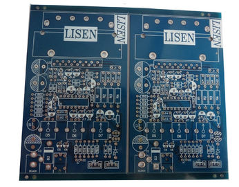
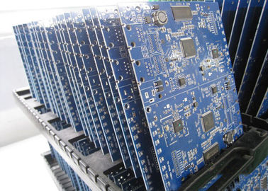
1oz LED Display Rigid PCB Board FR4 4 Layer Blue Soldermask
| PCB Name: |
LED Display PCB Board |
Layer count |
4 Layer |
| Base Material: |
FR4 |
Board Thickness: |
1.6mm |
| Copper Thickness: |
1oz |
Min. Hole Size: |
0.4mm |
| Min. Line Width/Spacing: |
0.15mm/0.15mm |
Surface treatment: |
Immersion Gold |
| Solder mask color: |
Blue |
Silkscreen color: |
White |
| Original: |
PCB Shenzhen House |
Service: |
PCB & PCBA |
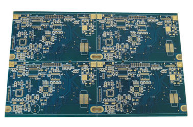
Description:
- Rigid PCB board for LED display
- FR4 PCB raw material
- PCB house with UL certificated
- Custom manufacturer PCB Shenzhen
- Single-sided, double side, alu PCB
China printing circuit board house specializes in PCB prototype and low volume PCB production manufacturing. Our printing circuit board manufacturing lines are located in China, which enable us to provide high quality, tight tolerance printed circuit boards at competitive prices.
From our printing circuit board, you are able to get instant contact with us to get online PCB quote only to tell us you requirement and send us PCB Gerber. Our team is waiting for you.
Applications:
Control Systems, LED Display, Digital Theater Systems, Vacuum Tube Electronics Displays, Linear Motors and Motion Products, Computer Diagnostic Tools, Lottery Pull-Tab and Scratch-off Ticket Machines, Point-of- Sale (POS) Electronic Security Systems, Automated ITVMs (Ticket Machines), Self-Service ATMs and Kiosks, Security Door Controls, Door Card Control, Electronic Lock, Aircraft Parts/Equipment, Switching Systems, Terminal Equipment, Publicly Accessible Equipment Vending Machines, Precision Positioning Systems, Robotics System, Water Purification System, Antenna, Guitar Electronics, Position Indicators, Controllers, Memory and Non-Memory Products, Networking, Wireless Communications ect.
Specification:
|
Layer count
|
Single sided, 2L, 4L,6L,8L,10L-26 Layers
|
|
Base material
|
FR4, High Tg FR4, CEM-3, Aluminum Base, Copper core, High frequency, Polyimide (PI), Polyester(PET) ,Rogers RO4350,Polyimide,Teflon,Getek Copper Clad Thermal Substrates
|
|
Board thickness
|
0.2mm, 0.4mm, 0.8mm, 1.0mm. 1.2mm.1.6mm.2.0mm-2.4mm, 3.2mm,4.0mm
|
|
Maximum Board Size
|
580mmx700mm
|
|
Copper thickness
|
0.5oz, 1oz, 2oz ,3oz., 4oz,5oz,6oz
|
|
Minimum Hole Size
|
0.2mm
|
|
Minimum Trace/Space
|
4mil/4mil
|
|
Surface finish
|
HASL(Hot Air Solder Level), Pb Free HASL , Electroless Nickel and Immersion Gold (ENIG), Plating Gold, Gold Fingers (Gold Connector), Silver Immersion, Organic Surface Protectant (OSP), Electroless Nickel Electroless Palladium Immersion Gold (ENEPIG),Hard Gold
|
|
Solder Mask
|
Green, Red, Blue, Black, Matte Green, Orange
|
|
Silk Screen
|
White, Yellow, Black
|
|
PCB Fabrication
|
Scoring, Route, V-Score, Counter Sink, Bevel, Cutouts and Slots
|
|
Quality Control
|
IPC 6012 Class 2, Electrical Testing, Flying probe Testing, 100% Netlist Testing
|
|
Special Technology
|
Impendence Control, Differencial PCB printed circuit board, Peelabemask PCB , High Density PCB HDI, Carbon Ink Printing,Heavy copper PCB ,Metal Core circuit boards ,Copper Clad PCB printed wiring board, Blind & Buried Vias, Laser Drilled Vias, Burn-in Boards,Backplanes, Bonded heat sinks, Controlled depth drilling, Controlled Impedance, Filled/plugged vias, Heavy copper, HDI, Large format PCB, Landless vias, Printed Electronics, RF
|
Advantage:
1. We offer low-cost PCB prototypes. No minimum order limit.
2. Fast quotation, 24 hour prompt response.
3. Our PCB factory is ISO/TS approved and with high & advanced production capabilities.
4. We are full service provider. Our services include PCB manufacturing, PCB assembly, components sourcing, stencil, also PCB layout, from specification to final production turnkey service. It is your good choice for one stop PCB solutions.
5. We provide technical and professional support, satisfactory customer service.
Contact us with your detail PCB requirement Now!

 يجب أن تكون رسالتك بين 20-3000 حرف!